For complex many layered geometries can require a long time to generate. 12 Filters two SMD as HFSS 3D Components one Laminate 1.

How To Define Electronics System In Hfss 3d Layout Youtube
Planar EM Slot Patch Antenna Created Date.

. Component Creation via Scripted Automation 7x faster 3D. Tianjian Lu ECE 546. This webinar series shows you how the HFSS adaptive meshing technology handles massive PCB layout geometries and gives you the most.
When a Wave Ports edge touches a radiation boundary the edges boundary is defined as PEC. It is named HFSSDesignn by default where n is the order in which the design was added to the project. Starts with a 3D surface triangular mesh on all objects and generate a 3D volume mesh throughout simulation domain Availability.
The base HFSS offering includes 3D and Layout interfaces 25D Method of Moments Eigenmode and Linear circuit simulation. Intro to Ansys HFSS 3D Layout Lesson 1. 1 On the Project menu click Insert HFSS Design The new design is listed in the project tree.
HFSS - 3D Layout Guides. Getting Started with HFSS 3D Layout. Cm Click the OK button Set Default Material To set the default material.
21m Layout w Mesh Assembly. It supports various layout formats generated in other major ECAD systems for analysis using the HFSS solver. 3D view for CAD 3D Layout view for ECAD such as Cadence Mentor Graphics August 16 2018 5 HFSS R19 User Interface within Ansys.
This video shows how to assign a solution setup for a cut out subdesign of the Intel Galileo board and then perform post processing operations after simulati. The Ansys HFSS 3D Layout course for printed circuit board design focuses on layered structures using the 3D Layout design type in HFSS and AEDT Ansys Electronic Desktop. Import your layout geometry from any PCB tool into HFSS easily.
This lesson introduces the tool and covers the interface details. The advanced-feature models along with electromagnetic layout analysis results in very accurate model-to-measurement agreement and fewer design iterations. I have done the design using HFSS 3D Design environment where I individually created each layer and stacking them manually about 40 layers total.
HFSS 3D Layout only Pro. 2m Validation. High Frequency Structure Simulator for 3D Electromagenetics HFSS is a platform that includes multiple simulation technologies for component or system design.
Start All Programs ANSYS Electromagnetics HFSS 150 Windows 64-bit or 32-bit HFSS 150 Set HFSS options. To open HFSS using the Windows search bar type in ANSYS Electronics Desktop The program itself is not actually called HFSS This is what the logo should look like. Sweep mesh in stackup z direction to generate tetrahedral mesh elements Advantage.
The outline for this workshop is as follows. I have designed a 24 GHz rectangular antenna on HFSS 3D model and got desired results while desing the same antenna with same dimensions I am getting resonance frequency at 27 GHz. This workshop covers the simulation aspects of ESD board modeling in HFSS 3D layout and its analysis.
Full-wave 3D EM models are now included in the library. Hfss 3d layout design tutorial New and most current patterns are increasingly being released by professionals so An increasing number of ladies can Adhere to the streak of nail art. Extremely fast relative to classic 3D mesh approach Con.
Problem Description Getting Started Create the 3D model Analysis Setup Plot S-parameters vs. Place and connect components in Layout Simulate components with 3D accuracy ECAD and MCAD HFSS SIwave Q3D. 12112019 122944 AM.
Only works for stack-up or swept in Z geometries. De ne variables HFSS Design Properties add r pad 075 mm t pad 01 mm as the radius and the thickness of the via pad respectively. Designed for brand new users this course covers layer stackup layout viewing ports vias simulation boundary extents layout driven assembly and hierarchy.
Getting Started with HFSS. 9m Validation 13m Layout w Mesh Assembly. Ansys High Frequency Structure Simulator HFSS Tutorial August 16 2018 1 MARK JONES PACIFIC NORTHWEST NATIONAL LABORATORY 82118.
When I compare both results they. I am thinking that I might missing some importent step while designing. HFSS Meshing Techniques Classic Approach.
High accuracy scalable parasitic models into the HFSS design environment makes EM co-simulation a seamless process. Hi I am trying to design a stackup layer consisting of metals and dielectrics in HFSS. Our Promise There is no PCB Package IC complexity that HFSS 3D Layout cannot solve.
Assembly Creation 5x faster 3D. When I compare both results they are very much different. Skips heavyweight ACIS and 3D surface mesh generation Availability.
Hi everyone I have design a 2x14 array by using HFSS 3D module and then exported the designed as dxf format and imported it in HFSS layout. Apply automated circuit simulation to capture full system behavior. Workshops include a small.
You cannot miss out on using HFSS on your complex layout geometries. It is analogous to the terminal solution type in HFSS. As you can imagine this was very time consuming about 6 hours.
Ease-of-use drive 3D simulation for design engineers. Works for any arbitrary 3D geometry Con. Do any one have a tutorial for designing microstrip antenna in HFSS 3D layout module.
3m LaminateBAW SMD 2. Upon opening HFSS you will see the screen below. From a layout generate layer by layer 2D triangular mesh.
Currently I am unfolding before you 12 easy 3D nail artwork designs ideas trends stickers. HFSS places a boundary condition on the Wave Ports edges to make sure the 2D eigenmode solution is finite sized Typically the edge boundary takes the boundary condition defined in the 3D geometry. HFSS traditional 3D interface and HFSS 3D Layout Pro.
Ansys HFSS 3D layout is a design type within the Ansys HFSS product. Layout-Driven Assembly in ANSYS Electronics Desktop. The 3D Modeler window appears to the right of the Project Manager.
如何在HFSS 3D佈局中構建和模擬微帶線HFSS 3D Layout是平面佈局設計環境 我們需要首先定義基板的疊層然後在每層上構建佈局. Click ModelerUnits Set Model Units. Project Opening 5x faster 3D.
August 16 2018 2. I - Insert an HFSS design into a project. Restore archive file comprising setup and analysis validate the design analyze the design view the results.
Hfss 3d Layout Design Tutorial. 1 Using the 3D Modeler Materials toolbar choose Select. Tools Options HFSS Options General Tab Check Use Wizards for data input when creating new boundaries Check Duplicate boundariesmesh operations with geometry Click OK.
Hi everyone I have design a 2x14 array by using HFSS 3D module and then exported the designed as dxf format and imported it in HFSS layout. The 3D models. Probe Feed Patch Antenna Probe Feed Patch Antenna -3 2 Choose Driven Terminal 3 Click the OK button Set Model Units To set the units.
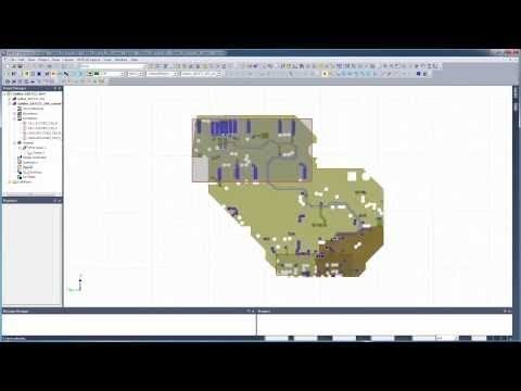
Ansys Hfss 3d Layout Cut Out Sub Design Simulation And Post Processing Youtube

Transient Time Domain Solutions From Hfss 3d Layout Youtube

How To Build And Simulate Microstrip In Hfss 3d Layout Youtube

How To Model Vias Of High Speed Differential Pairs With Hfss In Siwave Simulation Youtube
How To Build Components In Hfss 3d Layout Youtube

Ansys Hfss 3d Layout Model From A Cadence Board File Youtube

Ansys Hfss 3d Layout Model From A Cadence Board File Youtube

How To Plot Em Field In Hfss 3d Layout Youtube
0 comments
Post a Comment